Tailoring 2D semiconductor heterostructures with specific bandgaps is a key aspect of leveraging new quantum materials for electronics and optoelectronics, one of the hot topics for researchers currently working in nanotech. Craig Wall, applications scientist at Montana Instruments, recently investigated the subject using Mountains® software to analyze results from Raman spectroscopy and photoluminescence.

2D heterostructure assembly in a variable temperature environment
The basic heterostructure assembly principle is simple: exfoliate, for example, a monolayer of MoS2 (molybdenum disulfide), put it on top of another mono- or few- layer crystal, such as WS2 (tungsten disufide), add another 2D crystal, and so on. The resulting heterostructure represents an artificial material assembled in a specified sequence with single layer precision, held together by van der Waals forces.
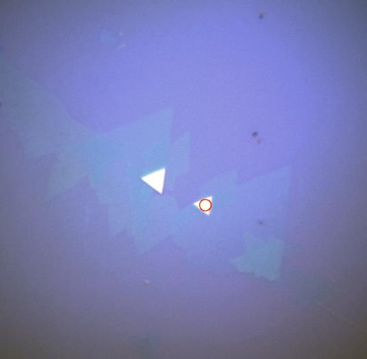
Figure 1. White light image of MoS2WS2 multilayer heterostructure
Often, additional or new information about a sample can be revealed with temperaturedependent measurements. In this study, we were able to demonstrate efficient hyperspectral mapping of 2D materials with the microReveal Raman spectroscopy and photoluminescence platform which maintains high spatial resolution and collection efficiency across the entire temperature range (4K to 500K). The system overcomes challenges associated with variable temperature sample drift by incorporating a low thermal mass sample stage, in-vacuum high NA objective, and coupling optics to a low astigmatism, broadband spectrograph.
The exciton recombination dynamics of stacked MoS2-WS2 heterostructures have previously been studied at room temperature.1-2 The maximum of the valence band and the minimum of the conduction band are separated in the layers of WS2 and MoS2, respectively. The reported energy gap for MoS2 is 2.39eV and for WS2 is 2.31eV. The energy difference between the maximum valence bands of MoS2 and WS2 is about 350 meV. Photoexcited free electron–hole pairs prefer to stay separated at layer interfaces. The excited electrons in WS2 tend to accumulate in the conduction band of MoS2 while holes generated in the valence band of MoS2 tend to transfer to WS2 at the interface. The interlayer radiative recombination of spatially separated carriers can lead to the extra peaks in the photoluminescence spectra. In our investigations, we were able to observe the interlayer exciton in the hyperspectral mapping study which is at lower energy compared with pure monolayer MoS2 and WS2.
Conclusions
Thermomechanical drift and stability become more complex to control when systematically varying temperature throughout an experiment. The hyperspectral maps (see below) are 200μm x 200μm with 1μm pixels and the collection of the 40,000 spectra that compose each map necessitates ultra-low thermomechanical drift, achievable with the microReveal. Studies of the epitaxial and non-epitaxial heterostructures of MoS2-WS2 on silicon suggest that interlayer exciton relaxation is independent of stacking epitaxy and orientation, see Fig. 13. For the non-epitaxial heterostructures, raising the temperature from 5K to 150K revealed edge effects on the intensity of the PL from the base WS2 layer.
Hyperspectral photoluminescence maps
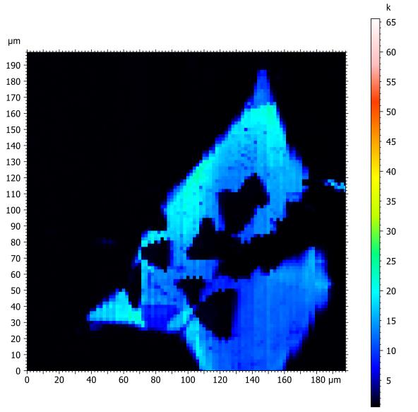
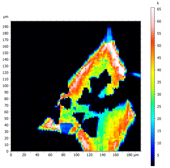
Above. Non-epitaxial MoS2-WS2 at 5K. Above. Non-epitaxial MoS2-WS2 at 150K.
Principal component analysis
with k means clustering illustrating unique spectral contributions
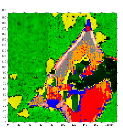

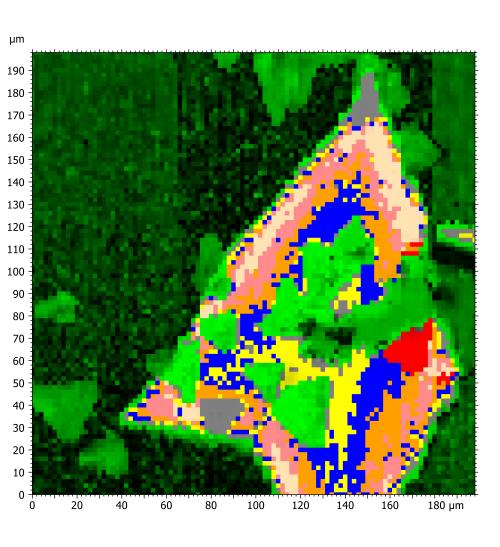
Above. Non-epitaxial MoS2-WS2 at 5K. Above. Non-epitaxial MoS2-WS2 at 150K.
Hyperspectral maps and advanced principal component analysis (PCA) were performed with Mountains® software.
References
1 J. Zhang, et. al., Observation of Strong Interlayer Coupling in MoS2/WS2 Heterostructures. Adv. Mater. 2016, 28, 1950–1956.
2 M. Thripuranthaka, et. al., Temperature dependent Raman spectroscopy of chemically derived few layer MoS2 and WS2 nanosheets. Appl. Phys. Lett. 2014, 104, 081911.
3 Y. Yifei, et. al., Equally Efficient Interlayer Exciton Relaxation and Improved Absorption in Epitaxial and Nonepitaxial MoS2/WS2 Heterostructures. Nano Lett. 2015, 15, 1, 486-491.
About Montana Instruments
Montana Instruments® Corporation designs and manufactures high-precision electrical, optical, and cryogenic systems for quantum materials research and the quantum computing, sensing and networking industries. Find out more: www.montanainstruments.com
Instruments & Sotware used
MicroReveal Raman spectroscopy and photoluminescence platform + MountainsLab® Premium (including Spectroscopy module) [Note, in version 9, these features are available in the MountainsSpectral® range].