In the last decades the need for clean energy has become an important issue due to global warming. Superconductors are one of the many potential solutions thanks to their ability to conduct electricity with zero energy loss. Atomic force microscopy (AFM), coupled with powerful analysis software, is the ideal tool for characterizing such materials.
A team from the Institut de Ciència de Materials de Barcelona (ICMAB-CSIC), Spain, used this technique in a recent study aiming to improve the performance of superconductor materials.
The importance of flat area fraction
REBa2Cu3O7 (RE – rare earth, Y) coated conductors have a multilayer architecture (figure 1) composed of a metallic substrate, several buffer layers, the REBCO layer and Cu and Ag protective layers.
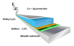
Figure 1. Architecture of a REBCO-coated conductor.
Zr-doped CeO2 (CZO) ultrathin layers (20-25 nm) are often used as cap layers for REBa2Cu3O7-x superconducting tapes, due to the low mismatch between their crystalline cell parameters. Therefore, surface characterization of the CZO layers is an important step before the deposition and growth of REBCO layers.
“We found that one of the key parameters that determine the surface quality of the buffer layers beyond roughness (Sq) is the flat area fraction1” explains Professor Teresa Puig, Head of the Superconducting Materials and Large-Scale Nanostructures Department at ICMAB. “With the help of atomic force microscopy (AFM) and MountainsSPIP® analysis software (formerly SPIPTM software), we were able to develop a methodology for determining the flat area fraction from topography measurements of the buffer layer surface.”
Determining the flat area fraction from topography
A morphological study of the CZO layer surface was performed using an Agilent 5100 atomic force microscope with AppNano silicon tips (FORT series, force applied 100nN) in tapping mode. Images were processed with MountainsSPIP® software. Besides roughness quantification, the software permits the calculation of the flat area fraction of the surface.
First, a threshold height value is defined, above which the surface is not considered flat. Usually, a three-unit cell of the structure is taken into consideration. In the case of the fluorite CZO, this is equivalent to ~1.5 nm. With this threshold value, a binary mask is applied to the whole AFM image. The result is a two-color image, where the flat area is represented in blue.
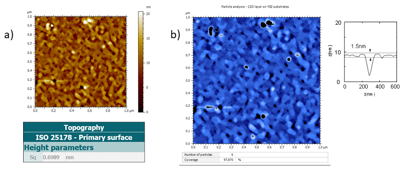
Figure 2. Root-mean-square roughness (a), flatness fraction (b) and profile through a typical line scan of the (a) (b) images of a 20 nm CZO layers grown on YSZ substrates, suitable for REBCO deposition.
CZO cap layers were grown on Yttria Stabilized Zirconia (YSZ) single crystals by metal organic decomposition (MOD). Figure 2 shows the surface characterization of CZO layers suitable for REBCO deposition (low Sq and high flat area fraction).
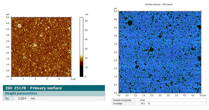
Figure 3. Root-mean-square roughness (a) & flatness fraction(b) of a 20 nm CZO layers grown on YSZ substrates unsuitable for REBCO deposition.
Figure 3 shows an example of CZO surfaces unsuitable for the deposition of REBCO layers (Sq > 2 nm and flat area fraction < 50 %).
Ready to try out our AFM image analysis software with your own data?
Conclusion: achieving better material performance
“With the help of MountainsSPIP® software we developed a method to determine the flat area fraction by designing a binary topography image map, from where to calculate accurately this parameter” concludes Teresa. “A thorough analysis of many film samples enabled us to assert that flat area fraction values above 50% result in YBCO textured films and that the higher these values are, the better. The software allowed us to investigate more deeply and understand the surface quality of our layers, and thus, to achieve better performances in our materials 2 3.”
References
1 Coll M, Pomar A, Puig T and Obradors X 2008 Atomically flat surface: The key issue for solution-derived epitaxial multilayers Appl. Phys. Express 1 1217011–3. DOI: 10.1143/APEX.1.121701
2 Pop C, Villarejo B, Pino F, Mundet B, Ricart S, De Palau M, Puig T and Obradors X 2019 Growth of all-chemical high critical current YBa 2 Cu 3 O 7-δ thick films and coated conductors, Supercond. Sci. Technol. 32, 015004. DOI: 10.1088/1361-6668/aaea4e
3 C.Pop, P. Barusco, R. Vlad, A. Queralto, K. Gupta, B. Almog, A. Saraf, G. Deutscher, X. Granados, T. Puig and X. Obradors 2022 High critical current solution derived YBa2Cu3O7 films grown on sapphire Supercond. Sci. Technol 35 054007. DOI: 10.1088/1361-6668/ac5be9
Authors

From left to right: Teresa Puig, Cornelia Pop, Mariona Coll, Xavier Obradors and Maite Simon at the Institut de Ciència de Materials de Barcelona, ICMAB-CISC.
Instruments and software used
Agilent 5100 AFM/SPM Microscope + MountainsSPIP® software.