The Institute of Electronics, Microelectronics and Nanotechnology (IEMN) in France, a research center with large-scale facilities dedicated to micro and nano fabrication processes, recently completed the “Dirac III-V” project investigating ways of producing Dirac electrons (electrons without any mass). This high-level project called for the use of many different fabrication and characterization methods as well as a software program capable of bringing together and processing the different kinds of datasets generated.
See the story in video (subtitles available):
Manufacturing a honeycomb array in an InGaAs quantum well
Molecular beam epitaxy (MBE) was used to grow a semiconductor quantum well, the main challenge being to turn this quantum well into an artificial honeycomb lattice by nanoperforating an array of pores at the limit of conventional lithographic techniques.
For that purpose, block copolymer lithography was used to produce a mask with a periodicity of 36nm. The pores were etched in the mask and into the SiO2 protecting layer.
After etching, scanning electron microscopy (SEM) was used to precisely check and quantify the geometry of the lattice and the degree of disorder which arises from the transfer of the microdomains which exist in the block copolymer film. The sample was then transferred into another etching machine to transfer the pores created in the mask to the InGaAs layer. Thus, a lattice of pores was created in the quantum well.
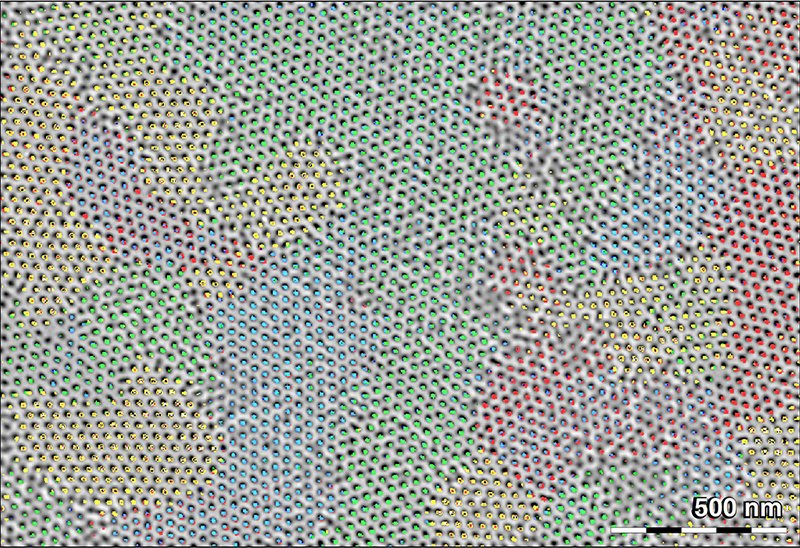
Above. The nanoperforated quantum well imaged using SEM to check the quality of the etching processes and examine the transfer of the grain boundaries of the block copolymer mask into the SiO2 protecting layer.
Multi-physical sample characterization
While the SEM produces high-resolution 2D (x,y) images allowing analysis of the lateral disorder in this two-dimensional structure, atomic force microscopy (AFM) was used to validate the etching processes by extracting vertical topographical information.
At this stage of the study, the surface of the sample was oxidized and transferred back to the MBE lab for cleaning and As capping which ensures a protection of the sample against air-exposure. X-Ray and UV photoelectron spectroscopy were used to characterize surface chemistry and investigate the bond structure of the sample.
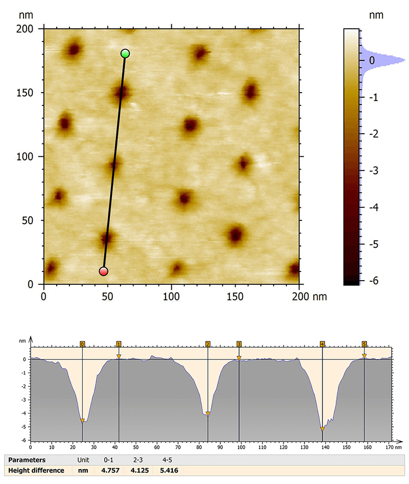
Above. AFM was used to obtain height information on the sample and check the depth of pores.
The Nanoprobe, a unique multi-physical instrument housed at the IEMN combining SEM, STM and spectroscopic techniques, was further used to measure the electrical resistivity of the native quantum well and the nanoperforated quantum well.
Above. The Nanoprobe instrument combines several technologies in itself: SEM, STM, optical spectroscopy etc.
“On this sample we wanted to probe the conductivity of a quantum well to ensure that the sample was compatible with lower temperature measurements” explains Maxime Berthe, SPM development engineer, “All the output measurements were analyzed together in one single software; Mountains® software allowed us to correlate our results.”
Finally, Scanning tunneling microscopy (STM), a surface-sensitive technique, was used to get accurate information about morphology and to resolve the outstanding electronic properties of the nanoperforated quantum well (in scanning tunneling spectroscopy mode).
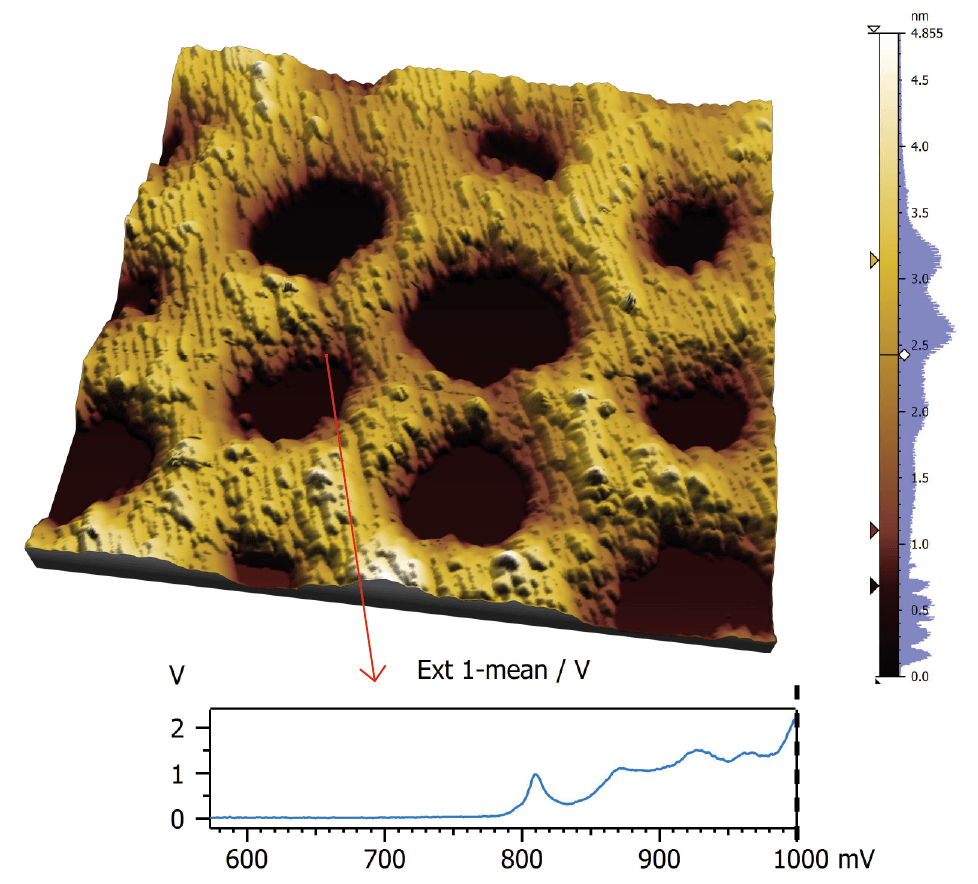
Above. Scanning tunneling spectroscopy (STS) data processing was performed using Mountains®.
“Once the measurements were completed and the data acquired, the next step was to extract some useful information and that’s where Mountains® software is very useful because we can process both topography and spectroscopy data in the same place.” reports Nemanja Peric, PhD researcher at IEMN.
Results
“The project was very challenging but rewarding when we were able to show the existence of specific electron states and finally the state we are looking for” concludes Bruno Grandidier, project leader. “Mountains® was key to processing the different nanofabrication steps involving multi-physical analysis and finally to prove the existence of electrons with very light mass.”
Read more
Engineering a Robust Flat Band in III–V Semiconductor Heterostructures, N. Franchina Vergel et al., Nano Lett. 2021, 21, 1, 680–685, Dec. 2020. doi.org/10.1021/acs.nanolett.0c04268
Instruments & software used
Scanning Electron Microscopy (SEM), Atomic Force Microscopy (AFM), Scanning Tunneling Microscopy (STM) (in scanning tunneling spectroscopy mode) + MountainsLab® software