Indium phosphide (InP) is a binary semiconductor used for instance in the fabrication of high-performance devices such as photodetectors and solar cells.
In a recent study led by an international research group, scientists from the Institut Supérieur de l’Électronique et du Numérique (ISEN) in Lille, France, investigated a new method for growing PbS nanoplatelets on sulfur-treated InP (001) surfaces. Scanning tunneling spectroscopy (STS), an extension of scanning tunneling microscopy (STM), and photoelectron spectroscopy were used to analyze results. Bruno Grandidier of the ISEN, tells us more.

Photo © Joaquim DASSONVILLE
Growing PbS Nanoplatelets on InP
“These nanoplatelets are usually made by immersing an InP substrate in a solution containing lead and selenium precursors.” explains Bruno Grandidier of the ISEN. “This is a low cost technique, easy to implement, but which has the disadvantage of generating interface defects between the nanocrystals and the semiconductor substrate. These defects greatly degrade the performance of optoelectronic components made from these heterostructures, such as photodetectors.”
A new fabrication method
“In our study, we were able to show that by chemically passivating the surface prior to the nanocrystalline growth, it is possible to produce non-degraded interfaces. The results of this can be seen directly on measurements made with scanning tunneling spectroscopy. Chemical and structural analyzes of the interfaces also show that their quality is comparable to the heterostructures produced in ultrahigh vacuum by molecular beam epitaxy (MBE).”
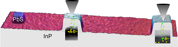
Above. Scanning tunneling spectroscopy demonstrated the difference in chemical composition and structure with and without chemical passivation of the InP surface (AFM image processed with Mountains® software).
Analyzing photoelectron spectroscopic measurements
“Several complementary methods were used to characterize the InP substrates in this study. In particular we used photoelectron spectroscopy to highlight the quality of the interfaces. By analyzing spectra produced we were able to confirm surface passivation thanks to the existence of two components in the S 2p core level, where the strongest component is caused by the In−S bonds and the smallest one being related to the Pb−S bonds in the nanoplatelets.”
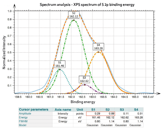
Above. XPS spectrum measured on PbS nanoplatelets grown on passivated InP substrates. The surface passivation is supported by the existence of two components in the S 2p core level, where the strongest component (S2) is caused by the In−S bonds and the smallest one (S1) being related to the Pb−S bonds in the nanoplatelets.
Instrument & software used
Scanning tunneling spectroscopy (STS) + MountainsSPIP® + Spectroscopy module, including the following Mountains® software tools: